


It’s not rocket science — it’s way more complex than that. Read this case study to learn how Micron not only pioneered but scaled the use of AI in our manufacturing, logistics and business processes to achieve technology leadership.
Micron does more than talk about artificial intelligence (AI). Using data analytics and AI in its own manufacturing processes, the company literally puts its money where its mouth is. It builds AI into the heart of its operations — demonstrating the value of the very technologies it enables with industry-leading memory and storage solutions.
Smart manufacturing goes beyond automation. It’s about intelligence that perceives, decides and improves — at scale. This includes everything from simulation and predictive analytics to machine learning and generative AI. Within this broader strategy, sensory AI and agentic AI play key roles: Sensory AI enables machines to “see, hear and feel” their environment through technologies like computer vision, acoustic listening and thermal imaging. Agentic AI systems interpret these inputs and act autonomously, learning continuously and coordinating across complex workflows.
Together, these capabilities support Micron’s transformative manufacturing strategy, enabling intelligent systems to detect anomalies, optimize processes and adapt in real time. The benefits are many: higher yields, safer working environments, greater efficiency, quicker time to market and a more sustainable business. This case study explores how Micron applies AI to one of the most complex engineering challenges in the world: manufacturing memory technologies on silicon wafers.
Complex manufacturing process
Micron’s factories produce memory technologies on silicon wafers through a highly complex and precise process, taking months and involving some 1,500 steps. The potential for error and for waste is high. But data and AI are helping to reduce that potential. When relying on human vigilance to spot and track flaws, mechanical problems and other trouble areas, the company lost time and money — losses that can be avoided with today’s sophisticated AI technologies to improve accuracy and coverage.
“We have built something here that is completely differentiated,” explains Koen de Backer, Micron corporate vice president of Smart Manufacturing & Artificial Intelligence. “We’re seeing much, much higher levels of accuracy. We can now launch products twice as fast — while saving 1 million work hours annually. It’s truly transformative.”

During the diffusion process, wafers have coatings evenly distributed across them. Each wafer is spun at high speeds (sometimes in a superheated environment) while material is added, causing the substance to spread across the surface with centrifugal force.
How Micron transforms wafers into leading-edge memory
The journey to advanced memory begins with silica — a type of sand, refined to 99.999% purity. This electronic-grade silicon is melted into ingots and sliced into ultra-thin wafers just 0.67 mm thick. Micron sources these electronic-grade wafers from specialized suppliers and processes them through our advanced fabrication systems to create high-performance memory chips.
At Micron’s cutting-edge manufacturing facilities, these sourced wafers undergo a series of precision-engineered steps — each designed to transform electronic-grade silicon into intelligent memory with microscopic accuracy.
- Polishing: Removes microscopic imperfections left from slicing the silicon ingot into wafers, ensuring a smooth surface for subsequent processing.
- Photoresist coating: Applies a light-sensitive material that enables precise patterning of circuitry through photolithography.
- Photolithography: Uses ultraviolet light to transfer intricate circuit designs onto the wafer, layer by layer, similar to photographic exposure.
- Doping and metallization: Alters the wafer’s electrical properties by introducing ionized plasma (doping) and adding conductive metal layers to form interconnects.
- Protective layering: Seals the wafer with a thin film to safeguard the circuitry during testing and handling.
- Testing and inspection: Validates functionality and structural integrity using AI-enhanced imaging and classification systems to detect flaws invisible to the human eye.
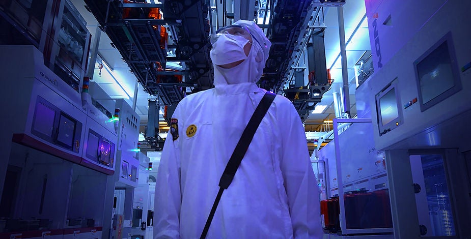
All of this takes place in sterile fabrication rooms — called cleanrooms — designed to prevent even the tiniest speck of dust from contaminating the pristine wafers. Yet despite these precautions, damage can still occur. Microscopic scratches, bubbles under the protective film or subtle structural flaws can compromise entire batches if left undetected.
Often, these flaws are microscopic — completely invisible to the naked eye. Even when they are visible, people scanning the 30 to 40 photos captured of each wafer during the photographic imaging process can overlook defects due to eye fatigue or momentary inattention. Blink, and the flaw is missed.
If issues aren’t caught until the test phase, a lot of time and money has already been wasted. Chances are the issue causing the flaw affects more than one wafer — possibly even thousands.
Other things can go wrong in production as well. Equipment parts wear out; pipes leak or drip hazardous chemicals onto products or people. Catching and correcting these issues early is imperative. Shutdowns are very expensive, leading to loss of revenue and missed productivity time. And given the complexities of semiconductor manufacturing, the many hours spent on recovery could put the true cost in the millions. What’s more, the risks associated with worker injuries are numerous. Finally, Micron’s commitment to sustainable and operational excellence drives us to make every process as energy-efficient and resilient as possible.
Detecting problems in products and machinery is vital for manufacturing efficiency, effectiveness and safety. Unfortunately, to err is human, and even the most highly trained person will not always see, hear or feel the very minute and subtle indicators that something is awry.
This is where AI steps in. AI systems detect subtle anomalies — scratches, bubbles, equipment wear — with laser-sharp precision and speed, far beyond human capability. AI systems collect petabytes of manufacturing data from more than 590,000 sources — feeding Micron’s cloud-based analytics environments to optimize production and catch issues in real time. These systems include computer vision, acoustic listening and thermal imaging — sensory AI capabilities that allow machines to perceive their environment.
Computer vision to see
The foundation of Micron’s AI-enabled manufacturing is image analytics. “Images are quite powerful in semiconductor manufacturing process,” explains Koen. “You can analyze detailed images of each step of the process.”
“By using AI computer vision and analyzing every stage,” he continues, “we can quickly identify any kind of deviation that happens — all in a completely automated way. This analysis spans everything — front end, assembly and test.”

Micron’s AI computer vision looks for potential flaws at the microscopic level throughout the entire fab and manufacturing process.
In addition to images, Micron employs video analytics to eliminate quality issues in assembly and testing. You may think video would be too data-intense to be practical. Yet Micron again uses AI to identify the critical moments to analyze. AI starts and stops the video stream to capture only the essential processes, keeping data size in check. Fortunately, Micron also builds the memory and storage devices that ensure this precious data is captured, retained and ready for use.
Imaging and video are especially effective, as wafer flaws come in many forms. For the most part, they fall into a few common categories: tiny holes near the wafer’s edge, scratches or bubbles in the outer film. Micron’s AI systems use computer vision technology to spot these defects on the images the photolithographic cameras capture as they etch circuitry onto the wafers during manufacturing.
Engineers direct the system to autonomously scan for tiny dots (holes) at the wafers’ edges, for instance, or for contiguous or slightly broken lines (scratches), or for color variations that signal dark or light spots. Some flaws are detected in near real time, with alerts triggered seconds after an image is taken. Other defects might be discovered during secondary scans minutes after the photographs are stored. All these processes rely on the AI system’s use of millions of images stored in the database environment for comparison and contrast.
The results have proven far more accurate than engineers’ assessments, as AI computer vision has higher accuracy and efficiency. Best of all, engineers can now focus on data collection and solving the root cause.
Micron’s AI automatic defect classification (ADC) system further streamlines this work. Technicians and engineers no longer need to classify wafer defects manually. Using deep learning, AI-ADC sorts and categorizes millions of flaws annually — learning and improving with each iteration. This form of machine learning clusters defects by type, helping engineers trace root causes and enabling AI systems to find flaws on their own and refine results.
Acoustic listening to hear
While AI imaging is at the core of the manufacturing process, Micron also employs acoustic listening to preempt issues. Abnormal sounds often signal a wearing part or an imminent breakdown.
Micron’s AI systems listen for anomalies in factory machinery via audial sensors installed strategically near robotic actuators or close to pumps. These microphones record normal activity for several weeks, and software converts the detected frequencies into graphs or charts depicting the sounds as visual data. When a new pitch or frequency appears, the system issues an alert. Often, it can even discern the cause of the anomaly.
Searching these massive databases can be time-consuming. When a machine is in danger of a breakdown, however, plant managers need to know immediately. Sending the data to an AI system filled with GPUs, accelerators and — importantly — Micron memory and storage, provide intelligent results much more quickly than CPU-based systems can. All these AI systems with hundreds of thousands of GPU cores and high-bandwidth memory working simultaneously and synergistically can refine their results in the blink of an eye with little or no human intervention. Plus, they can improve their diagnostics with each iteration.
Thermal imaging to feel
Not every malfunction makes noise — and in a manufacturing environment, silence can be deadly. Sometimes, the only warning is a change in temperature. Until recently, the only way to detect a temperature spike was to see a red glow, sparks or smoke. By the time this appeared, the problem had already entered the danger zone, and the plant needed to evacuate workers.
So, in addition to image analytics and acoustic listening, Micron also uses thermal imaging, which measures the temperature of key components.
“Temperature measurement on transformers is key to prevention of overheating,” Koen explains. “Early detection can make the difference between doing a simple repair and replacing an entire, expensive piece of equipment.”
Finally, these AI sensors for imagery, sound and temperature ultimately impact the company's bottom line. “These sensors excel for quality and efficiency improvements, but also for achieving cost saving,” Koen adds. “They deliver granular metering of energy, leading to significant usage and energy savings.”
The numbers
At Micron, 590,000 sensors produce 100 million wafer images in 436 million control points. All are run through AI models each week. In addition, 77 petabytes of data are stored, and 58 terabytes of new data are captured each day.
This scale of AI adoption supports applications in yield analytics, digital-twin planning, internet of things (IoT) and image analytics, optimization and advanced algorithms, process automation and mobile applications.
The results1 are undeniable:
- 4% improvement in manufacturing tool availability
- 1 million work hours annually in labor productivity gains
- 50% reduction in time to market for new products
- 50% reduction in product scrap
And the benefits extend beyond the fab. AI now supports every aspect of Micron’s operations — from sales and marketing to human resources, business operations, research and development, and business systems.
“This is about transforming the enterprise, not just the shop floor,” Koen says. “We have brought AI to all business processes within our company.”
Ecosystem partnerships
Beyond optimizing the internal manufacturing process, Micron also uses AI while working directly with suppliers, giving them detailed feedback on their products to ensure the best energy efficiency. With these suppliers, Micron coordinates DIMS (data ingestion into Micron systems) so that ingestion happens at the highest frequencies. Micron engineers monitor this ingestion in real time. Likewise, correction and optimization are constantly taking place at extremely granular levels.
In addition, Micron uses telemetry data to measure the effect of its products in suppliers’ data centers. This data, combined with internal data, underpins real-time collaboration to improve products for their specific workloads.
Micron also closely monitors the performance of its models. Using AI on incoming data and retraining allows engineers to focus on automating the machine learning flow. Otherwise, there would never be enough data scientists to keep up, and they’d be chasing events that have already happened.
These initiatives are backed by an internal data science academy and continued investment in in-house data scientists, engineers and solution architects. These resources, along with Micron’s citizen data science model, enable functional experts to use Al-powered tools and insights.
Industry leadership
Today, Micron combines a rich heritage of core process knowledge with the unparalleled efficiencies of AI. Data experts have created large yield-management platforms used by more than 14,000 people across the company. At the same time, dedicated teams focused on day-to-day yield optimization are building new prototypes in fast integration cycles. These prototypes are frequently implemented to optimize major platforms.
Thanks to the dedication of Micron team members and its advanced, AI-enhanced manufacturing processes, the company has achieved record-breaking yields across multiple generations of memory technology. Its latest innovations reached mature yields faster than previous generations, underscoring the strength of its engineering and operational excellence — and reinforcing Micron’s position as a technology leader.
Micron has optimized AI in manufacturing not just as a tool, but as a system of intelligence that has transformed the process. But what truly sets the company apart is how its implementation of AI at scale is also transforming the enterprise. From simulation and predictive analytics to machine learning, generative AI and real-time process optimization, Micron’s AI strategy touches every corner of the business. Far from taking everyone’s jobs, this new technology is augmenting and empowering teams that no longer focus on acquiring data and doing multiple base analyses. Now they can focus on what they’re good at — innovating to develop industry-leading products and business practices.
1 Improvements based on Micron internal data and analysis gathered from 2016 through 2025
