


The automotive challenge
Micron Technology has been the global leader in memory and storage solutions in the automotive market for over 30 years. This success builds on our innovation and close collaboration with the ecosystem of automotive SoC vendors, OEMs and tier 1 suppliers. Memory and storage are foundational to many innovations in automotive electronics architectures. Fine-tuning our product capabilities and delivering the right product for the right application has historically improved vehicle quality and end-user experiences. Examples through the years span from designing for quality, adding burn-in to reduce infant mortality rates, increasing temperature during test to match automotive environments, receiving certifications for product use in functional safety (FuSa) relevant applications and enhancing device features to meet the vehicle designer’s system needs.
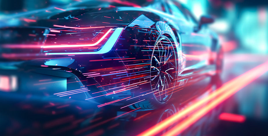
Applications in advanced driver assistance systems (ADAS) and in-vehicle entertainment (IVE) continue to challenge the industry to deliver higher performance systems. Key factors driving this performance need in IVI multiple 4K/8K screens, in-cabin sensing for driver and passenger needs, and generative artificial intelligence (AI) processing locally. ADAS systems have deployed machine learning and AI to achieve higher safety levels (level 2, 2+, 3 and above). The amount of data to be analyzed with decision-making capability is amplified by the increased number of sensors and higher resolution cameras (L2/L2+ = 25-30 sensing touchpoints)1. All these requirements need fast memory and processors to analyze large data streams, interpret them correctly and make split-second decisions. This complexity is driving the need for up to 300-500 GB/s bandwidth2. After collaborating with customers and joining forces with targeted silicon intellectual property (IP) providers and chip set vendors (automotive processor suppliers), Micron has developed an enhanced LPDDR5X product designed for optimum performance in automotive platforms.
Addressing the system need
Our groundbreaking LPDDR5X-optimized error correction code (ECC) scheme mitigates all system in-line ECC penalties delivering a 15% to 25%3 bandwidth increase. This new LPDDR5X-optimized ECC scheme, called direct link ECC protocol (DLEP), not only delivers increased performance but also helps LPDDR5X memory systems achieve the ISO 26262 ASIL-D hardware metric through reduced failures in time (FIT). Additionally, this new product delivers approximately 10% lower power consumption on a pJ/b (picojoule-per-bit) perspective and a minimum 6% additional addressable memory space4. Built on the backbone of Micron’s certified ISO 26262 ASIL-D systematic LPDDR5X DRAM, critical automotive FuSa requirements are now readily achievable.
Our new LPDDR5X DRAM with DLEP is JEDEC compatible and designed to meet the stringent demands of automotive applications, offering a product life cycle of over five years and the ability to operate at extreme temperature ranges. This new DLEP-enhanced DRAM offers greater value by providing the increased bandwidth required by high-performance applications. DLEP-enabled LPDDR5X DRAM is another example of Micron’s continuous innovation and ability to drive solutions that solve memory and storage challenges for the automotive market. Ultimately, we expect this product, with higher bandwidth and lower power, will deliver a lower total cost of ownership (TCO) to our customers.
Looking ahead of the curve
Some may be asking what’s next, how does it work or how do I get DLEP-enabled LPDDR5X DRAM? In the near future, you will hear from our SoC (system-on-chip) and IP partners as they launch their hardware and IP blocks. These announcements will come after countless hours of collaboration with our SoC partners and the selection of the best solution for our customers. The beauty of the solution is that the connection between the DRAM and processor does the work to drive performance. This type of collaboration enables Micron and its partners to deliver faster time to market, better products and cost savings for customers. A system that is properly configured using LPDDR5X with DLEP DRAM could drive additional savings of millions of dollars over the lifetime of the platform through SoC silicon die savings and SoC board size reduction, using both smaller packages and fewer components overall5. Lastly, these high-end LPDDR5X devices are available now and as part of our functional safety program can be identified with the “FAIT”, “FAAT” and “FAUT” part number designators. These LPDDR5X with DLEP products will enable automotive systems for many years. At Micron, we celebrate great wins and continue looking for the next problem to solve. As we look around the corner, we see AI and data-rich content becoming more complex, with memory and storage central to the solution.
1 Data size and bandwidth are estimated based on industry standards ISO 23150 & Autosar Specification of Sensor Interfaces (R20-11). Sensor examples go from LiDAR to cameras to GPS to ultrasonic sensors.
2 Based on sensor needs and 8bit-LLMs, assumes GGML quantization: ggml.ai | PIM: Processing-in-memory S. Kim, et al. "Full stack optimization of transformer inference: a survey." arXiv preprint arXiv:2302.14017 (2023).
3 Measured against typical in-line system ECC schemes vs. DLEP
4 “additional addressable memory space” based on recovered memory density used to store system ECC parity
5 Based on a standard system requiring 512 I/Os for DRAM vs. a LPDDR5X w/ DLEP DRAM system requiring only 416 I/Os for an equivalent 500GB/s.
